As every manufacturer, regardless of size or sector, faces increasing demands on both time and budget they need to find smarter ways of developing and delivering their end products. So why would you make your own PCBs, asks Newbury Electronics
Smart engineering processes and solutions that are connected and allow us to harness the power of the Internet are not always the panacea they may at first seem. Sometimes simply taking a shrewder approach to your procurement may deliver equally, but hitherto, unseen valuable benefits.
One obvious crucial area where outsourcing can save not only time and money but also arguably supply a higher quality end product is contract assembly PCBs. As boards and the electronics which they house becoming increasingly complex it is no longer viable for each and every manufacturer to have its own in house electrical design and production department. Few, if any, organisations would ever see a decent return on their investment if they were to purchase the necessary plant and equipment to deliver the boards to the standard required in today's manufacturing environment.
They need to turn to specialist suppliers for whom board PCB assembly is the mainstay of their business and who understand the benefit of capital investment to keep them at the forefront of their chosen area of specialisation. Companies like this invest not only in the latest equipment, but also have the knowledge and understanding of the latest processes, materials and methods and will provide their customers with design guidance, technical support and then deliver the boards to meet both the time and budget restraints.
Real benefits from a specialist
So where will a specialist PCB assembler be making their investment in the 21st century?
There are seven key areas where a specialist provider can deliver real benefit to their customer;
1. Automated first article inspection – checking that you have it right at the earliest stages and making any corrections that may be required there and then incurs far lower costs than discovering a boarding error at a later stage of the process where project delays can have serious economic implications.
2. In house solder paste stencil manufacture – it is well understood in the industry that the quality of the initial stencil impacts on the final board, and many regard this as the pivotal stage in the entire process. Mistakes can and do occur but it is far quicker and easier to rectify a faulty stencil on-site where you are familiar with all elements of the project than having to involve a third party where neither the end client of the assembler can be entirely confident about what has been included.
3. Vapour phase reflow – This is a high-quality method of reflow soldering. Every PCB assembly will have its own unique reflow profile requirement. When convection reflow is troublesome to successfully qualify, vapour phase reflow is preferred being far more tolerant of thermal mass variation with a far wider operating window. It is the reflow process of choice.
4. 3D AOI (Automated Optical Inspection) – as with Point 1, first article inspection, maintaining the highest quality throughout the process and identifying any potential problems as the earliest opportunity delivers a smoother production process. The high-resolution capabilities of these machine inspection tools supersede the capabilities of the human eye and in effect the equipment is able to 'learn' as it inspects.
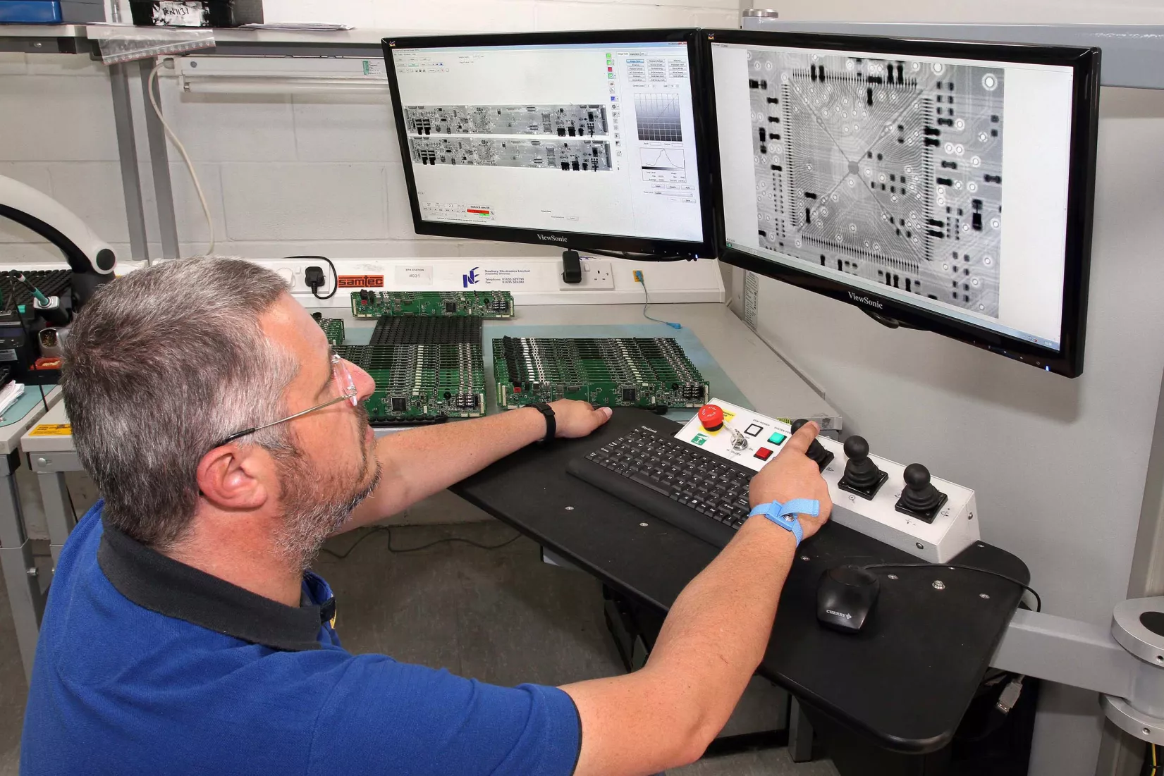
5. X-ray inspection – as boards become increasingly complex, many of the connections will be hidden from view underneath the board's components, making X-ray examination the only viable option.
6. Robotic selective soldering of lead-in parts – whilst manual soldering has long been a mainstay of board assembly this has inevitably had an element of variability. With robotic solutions quality is maintained and smaller and more complex joints can be handled with ease.
7. In-house bare-board manufacture – with so much of CEM being automated, bare PCBs must be presented in step & repeated carrier pallets which can be automatically handled through pick & place, AOI, and selective soldering. A CEM with access to in-house bare PCB manufacture will ensure that DFM (design for manufacturing) is designed in from the start
The capital investment required to acquire the latest equipment to cope with the processes described above is out of reach of any but those for whom PCBs are the bread and butter of their business. By contracting out the engineering design and the manufacture many large organisations have already achieved internal efficiencies. Using an agile and dynamic supplier that understands both the mechanical and electrical elements of the work and who is able to apply this technology and knowledge is definitely the way forward, and makes both business and engineering sense.